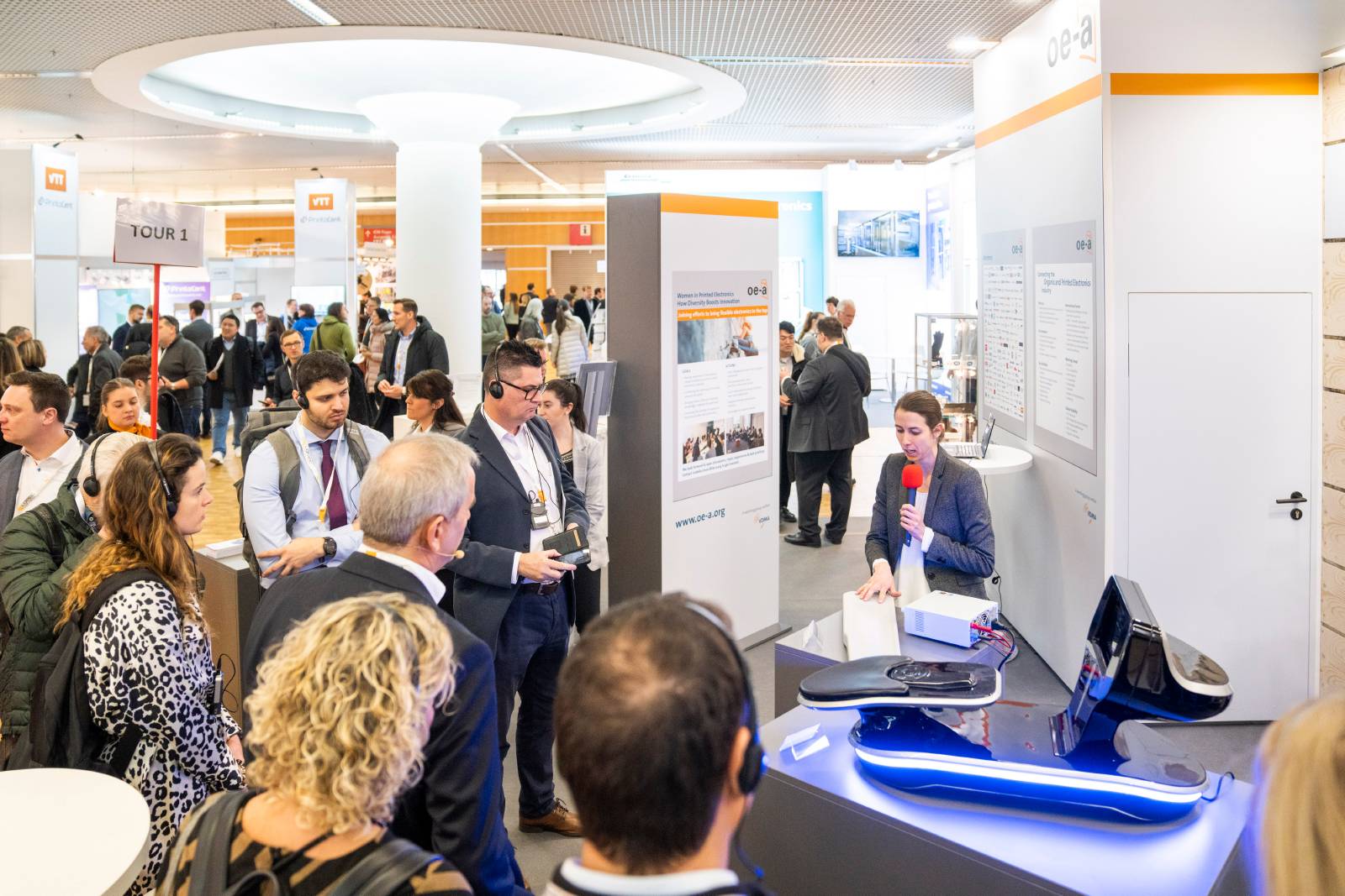


Hahn-Schickard, Germany
In the manufacturing industry, the buzzwords IoT, digitalization, Industry 4.0, etc. are now omnipresent. The associated technological achievements will sustainably support and improve our society. However, the current production of electrical circuits and electronics is based on subtractive processes that consume large amounts of chemicals and produce large amounts of wastewater. Centralized mass production also leads to a large ecological footprint due to the long logistics routes. The overall goal of the project is therefore to provide a novel digital and resource-efficient additive manufacturing technology for hybrid multi-material components by combining high-performance dielectric material dispensing, FDM polymer printing, direct printing of molten conductive metal and soldering of functional units using StarJet technology on an open source 3D printing platform (AME).
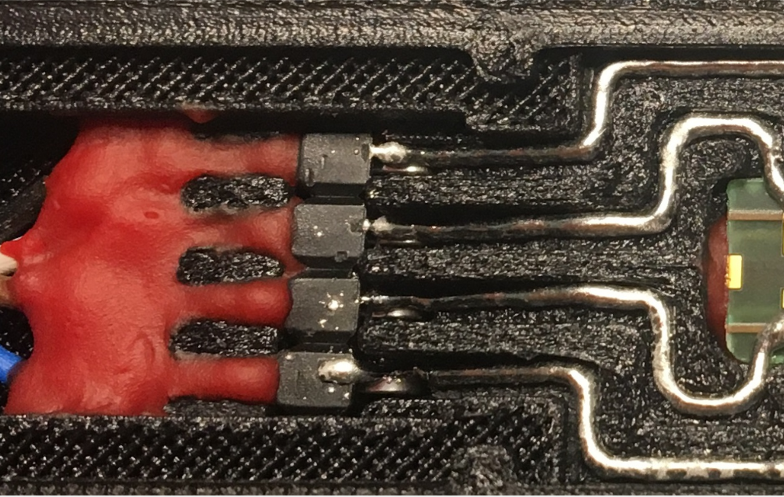
With molten metal printing (StarJet) of conductive tracks and selective connection of functional units (e.g. sensors, LEDs,microchips), much simpler processes and higher reliability (i.e. high adhesion and thermal stability on dielectrics) can be achieved compared to ink-based solutions. This is because 100% metal content, no solvent, no post-processing and no additional step for SMD assembly are used. Overall, the planned hybrid 3D electronic printing platform enables the direct additive manufacturing of electrical circuits and electronics as well as functional and customized intelligent components. Thanks to its small size and easy installation, it could also enable decentralized production of small to medium series, cost efficient design utilization and a fast design-product cycle for SMEs.
Functionality
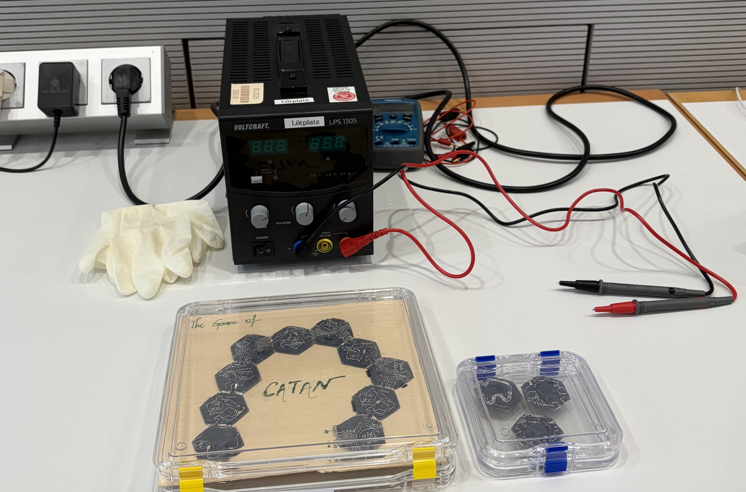
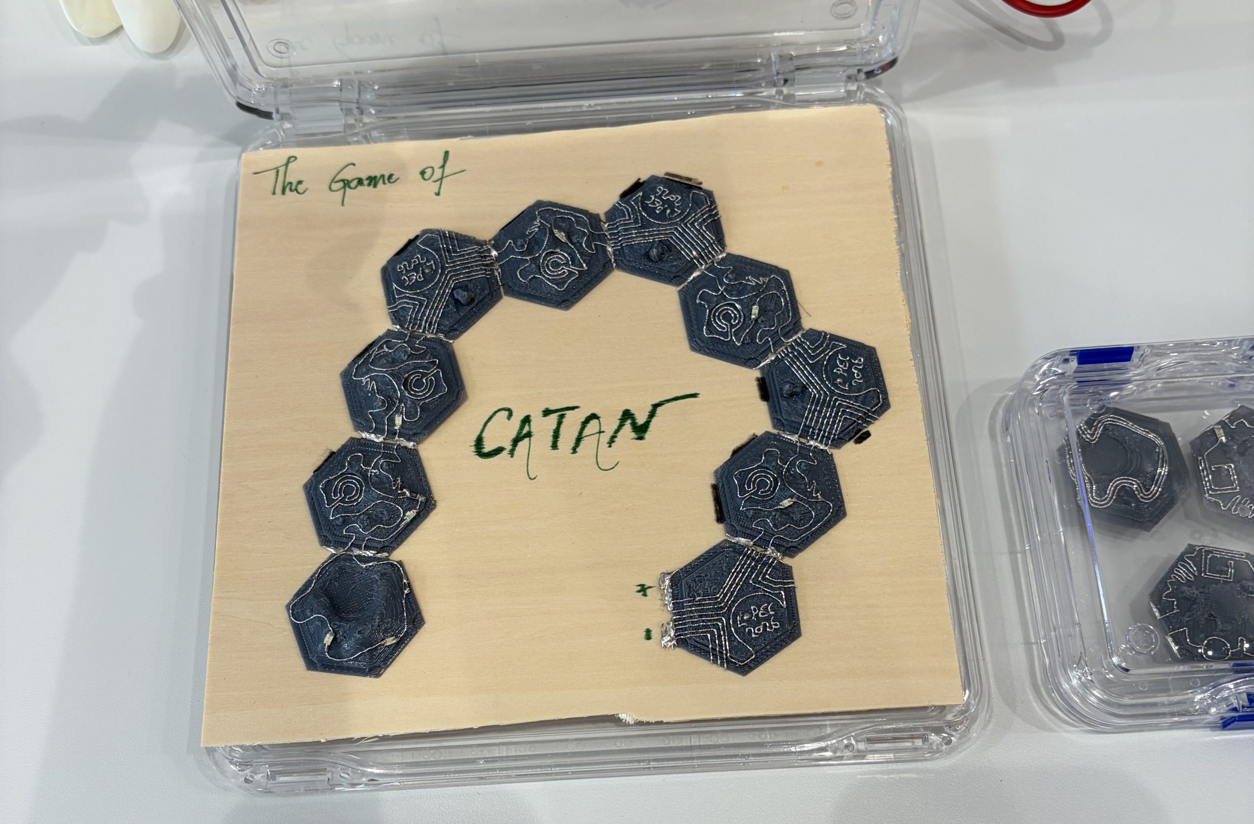
The demonstrator showcases the primary objective of the project: the capabilityto print dielectric materials, conductive paths, interconnections, and directlysolder surface-mounted devices (SMDs). To illustrate this, a racing car trackfeaturing initially disconnected conductive paths connected to LEDs will befabricated. The track will use Fused Filament Fabrication (FFF) for the dielectricsubstrate and the StarJet technology for the conductive pathways. When a carmoves along the track, dragging a piece of metal across the gaps, thepreviously disconnected paths will be completed, causing the LEDs toilluminate.
This simple yet effective demonstrator highlights the potential of additivemanufacturing for electronics by reducing its inherent complexity. Itdemonstrates how a complete electronic system can be fabricated from start tofinish on a single platform, achieving high performance through molten-metalconductive pathways.
Benefits of the Project
The project offers a transformative approach to the manufacturing of electronic components by enabling fully additive, resource-efficient production of hybrid multi-material systems. Traditional subtractive processes for electronics consume large amounts of chemicals, generate significant wastewater, and rely on centralized mass production, leading to long logistics routes and a substantial ecological footprint. In contrast, the proposed platform combines high-performance dielectric material dispensing, FDM polymer printing, and direct printing of molten metal conductive tracks with selective soldering of functional units using StarJet technology. This approach eliminates solvents, ensures 100% metal content, avoids post-processing, and integrates SMD assembly into a single step, resulting in higher reliability, improved adhesion, and superior thermal stability compared to ink-based methods. The hybrid process is further optimized through thermal simulations and the use of advanced dielectrics, while seamless integration with 3D electronics CAD/CAM workflows ensures precise, efficient fabrication. Overall, the platform enables direct additive manufacturing of electrical circuits, intelligent functional components, and customized devices, supporting decentralized production, small to medium series manufacturing, cost-efficient design utilization, and accelerated design-to-product cycles, particularly for SMEs.
Target Industry
- Consumer Electronics
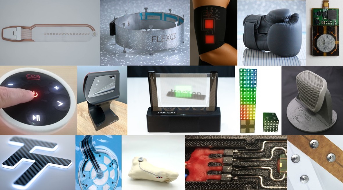
Organic & Printed Components
- Conductive path
- Interconnection
- Printed dielectric / insulator
- Direct soldering of SMD components
Classical Components
- Resistors
- LEDs